

Capacitor discharge welding (CDW) is an advanced joining technique that stands out for its speed, precision and efficiency. Unlike traditional resistance or arc welding, which rely on a continuous power source, CDW stores energy in a bank of capacitors and releases it in an intense burst lasting just a few milliseconds. This rapid discharge generates highly localised heat, enabling metals to bond in a solid state without melting or distorting the surrounding material. The result is a clean, reliable connection with minimal thermal impact. Thanks to its ability to join a wide range of conductive materials, including challenging combinations such as copper with aluminium or silver with brass, CDW is becoming increasingly valuable in modern manufacturing. The process eliminates the need for filler materials and preserves the microstructure of the components, making it particularly suitable for high-precision applications. This article presents an overview of how CDW works, covering everything from its electrical and mechanical systems to the thermal dynamics that govern the weld. The article also examines how engineers optimise parameters to achieve consistent results, highlighting the technology’s growing role in industries such as power electronics, where compact, low-resistance joints are essential for performance and reliability.
Introduction
Capacitor discharge welding (CDW) is a solid-state resistance welding process characterised by the use of a capacitive energy storage system to supply a short-duration, high-intensity current pulse through a joint interface. This process is also known as capacitance discharge or stored-energy resistance welding.
CDW is popular in industry due to its ability to deliver large current peaks (up to hundreds of kiloamperes) for extremely short times (typically 1–10 milliseconds). This allows a metallurgical bond to be formed with minimal heat diffusion into the surrounding material. Consequently, CDW can join thin sheets, fine electrical components, or hardened materials without altering their mechanical properties, coatings, or precision tolerances.
Early investigations demonstrated that CDW could produce continuous metallurgical bonds between similar and dissimilar metals, such as silver–brass or Fe-Al intermetallic. More recent developments, such as projection CDW for advanced alloys and supercapacitor-based energy storage systems, have further increased its industrial versatility, including the possibility to welt inox steel and aluminum alloy.
Today, CDW is used in several sectors, including electronics, automotive, nuclear and energy conversion systems, for tasks requiring precision, repeatability and limited thermal influence. Examples include the welding of battery tabs, busbars, terminals, connectors and sensor housings.
Process principle and energy transfer
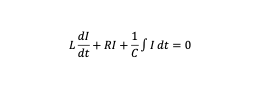
At its core, CDW involves the rapid release of stored electrical energy from a capacitor bank into a low-resistance circuit containing the workpieces. This circuit can be schematically represented by a charged capacitor (C), a discharge switch (e.g. a thyristor) and a resistive-inductive load consisting of cables, electrodes and the joint interface (figure 1).
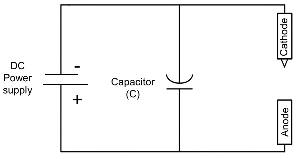
When the switch is closed, the capacitor discharges according to the following equation:

(1)
Where τ = L / R is the time constant of the discharge circuit, L is the inductance, and R is the total resistance. The stored energy, E = 1/2 CV2 is transformed into heat through Joule effect:
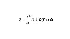
(2)
The waveform is typically oscillatory with a single dominant half-cycle, lasting 2–10 ms depending on the capacitance and circuit inductance. The peak current may exceed 1000 times the charging current of the capacitor bank, providing an instantaneous power density on the order of 10⁸–10⁹ W/m² at the contact interface.
Because resistance is concentrated at microscopic asperities, heating is confined to a thin surface layer (tens of micrometers). The result is localized softening or partial surface melting, which under applied pressure produces intimate metal-to-metal bonding without significant bulk melting.
This rapid process eliminates the need for external shielding gas or filler metal and minimizes oxidation. The total thermal cycle is shorter than the typical heat conduction time of metals, so the heat-affected zone (HAZ) is negligible (figure 2).
(credit: Corotrat srl)
Equipment and system architecture
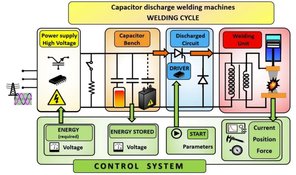
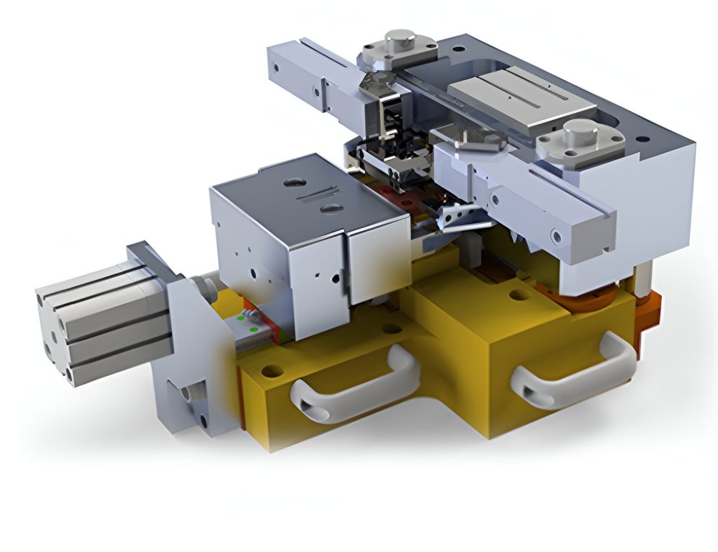
A CDW installation consists of three primary subsystems: the electrical power supply, the mechanical welding head, and the control and monitoring unit. The design of each subsystem must ensure synchronization between electrical discharge, pressure application, and joint deformation.
The power supply contains a transformer–rectifier unit for charging the capacitor bank, a capacitor bank for energy storage, and a switching device to initiate discharge.
- Capacitor Bank: Typically composed of electrolytic or pulse-rated film capacitors, with total capacitance between 100 µF and several millifarads. In modern systems, supercapacitors (electrochemical double-layer capacitors) are used, offering energy densities 10–100 times higher than conventional designs.
- Charging Voltage: Usually ranges from 10 V (microjoining) up to 400 V (heavy projection welding). The discharge energy E = 1/2 CV2 can vary from 5 J to 120.000 J.
- Discharge Switch: Early systems used spark gaps; current systems employ thyristors or insulated-gate bipolar transistors (IGBTs) capable of microsecond response and long service life.
- Transformer: Provides galvanic isolation and adapts voltage/current levels; the turns ratio defines the pulse amplitude and waveform shape.
- Secondary Circuit: Includes low-resistance copper busbars, flexible cables, and electrodes. Its total inductance must be minimized to avoid current delay and oscillation.
A typical circuit exhibits a pulse duration of 5-15 ms and a current rise time <1 ms. Because the capacitor bank is recharged during idle time, the power draw from the grid is low and nearly constant, improving energy efficiency (figure 3).
The mechanical subsystem ensures stable electrode alignment, force control, and rapid response during the discharge. Pneumatic, hydraulic, or servo-electric actuators apply the clamping force before firing and maintain pressure throughout the pulse.
Typical electrode forces range from:
- 50-500 N for small studs or terminals;
- 2-100 kN for projection CDW of larger components.
The follow-up system, often using Belleville spring stacks or servo-feedback actuators or elastomer, allows dynamic compensation for collapse of projections or material displacement during welding, maintaining contact pressure in the millisecond time frame.
A PLC-based control unit coordinates capacitor charging, pressure application, discharge triggering, and quality monitoring. Sensors record voltage, current, displacement, and force. Modern systems incorporate real-time waveform analysis to detect abnormal discharges, open circuits, or misalignment.
Safety interlocks prevent firing if the electrodes are not in contact or if the charge voltage exceeds set limits. Because of the high stored energy, discharge resistors are installed to safely bleed residual charge after each cycle.
Types of CDW processes
Capacitor Discharge Welding (CDW) encompasses several process variants, each tailored to specific industrial applications:
Projection Capacitor Discharge Welding (P-CDW), uses a geometric projection on one of the parts to concentrate current and pressure in a localized region. This approach is particularly effective for joining small-diameter tubes, rings, or electrical terminals. During welding, the projection collapses under pressure, promoting solid-state bonding without melting. The P-CDW configuration allows for highly repeatable energy distribution and makes it possible to join materials with markedly different thermal conductivities, such as ferritic stainless steels and oxide dispersion–strengthened alloys.
For high-precision joining of dissimilar materials, the initial gap and drawn-arc CDW variants are often preferred. In the initial gap method, a small separation between the components allows the establishment of a controlled plasma arc when the electrode descends. The drawn-arc version introduces electronic control to retract and reapply pressure during the discharge pulse, providing finer regulation of fusion depth and improved joint consistency.
Regardless of the specific configuration, the mechanism of heat generation and material behavior during CDW remains fundamentally similar. Most heat is generated at the contact interface, where the electrical resistance is highest. The temperature–time profile depends on current density, contact resistance, and the thermal properties of the materials involved. The heating rate can reach
K/s, far exceeding that of laser or electron beam welding, ensuring extremely rapid solidification or localized diffusion bonding. Ketzel et al. showed that metal vaporization and surface activation occur within the first millisecond of the discharge, followed by pressure-induced consolidation. Cross-sectional analyses typically reveal the absence of a classic weld nugget; instead, a continuous bonding zone forms through plastic deformation and solid-state diffusion.
The thermal conductivity and electrical resistivity of the materials strongly influence the required process parameters. Materials with high thermal conductivity, such as copper, demand higher stored energy or sharper projections to achieve sufficient interface temperatures. Conversely, alloys with lower thermal conductivity or higher resistivity, such as stainless steels or titanium, require less energy to prevent melting and maintain solid-state bonding conditions. Process windows are typically determined through experimental calibration. For instance, Lienert et al. identified stable parameter ranges for ferritic stainless steel in the range of 350–600 J and electrode forces between 2-4 kN, achieving displacements of 150–300 µm without evidence of melting.
Overall, these CDW variants illustrate the process’s versatility and controllability, enabling reliable solid-state or shallow-fusion bonding across a wide spectrum of materials and geometries.
Heat generation and material behavior
During CDW, most heat is produced at the contact interface where the electrical resistance is highest. The temperature–time profile depends on current density, contact resistance, and material thermal properties.
The heating rate can reach 10⁶–10⁸ K/s, exceeding rates in laser or electron beam welding. The resulting high temperature gradient ensures rapid solidification or localized diffusion bonding.
Ketzel et al. demonstrated that metal vaporization and surface activation occur during the first millisecond of discharge, followed by pressure-induced consolidation. Cross-section analysis shows absence of a classic “weld nugget”; instead, a continuous bonding zone forms through plastic deformation and solid-state diffusion.
For materials with high thermal conductivity (e.g., copper), higher stored energy or sharper projections are required to achieve adequate interface temperature. Conversely, alloys with low thermal conductivity or high resistivity (e.g., stainless steels, titanium) require lower energy to avoid melting.
Process windows are typically determined experimentally. For example, Lienert et al. identified stable parameter ranges for ferritic stainless steel at 350-600 J and electrode forces of 2-4 kN, achieving displacements of 150–300 µm without melting.
Process modeling and parameter interaction
Analytical and numerical modeling play a crucial role in understanding the coupled thermal, electrical, and mechanical phenomena involved in Capacitor Discharge Welding (CDW).
Electrical Modeling:
By considering a lumped circuit characterized by a total resistance R and inductance L, the discharge process can be described by the differential equation:
(3)
which yields a damped oscillatory current. The pulse shape is governed by the natural frequency
ω0 = 1/ √LC and the damping factor ζ = R / √L/C. Minimizing both and
increases the peak current and enhances the efficiency of energy transfer to the joint.
Thermal Modeling:
The instantaneous power density is expressed as:

(4)
where is the current density and
the electrical resistivity. Finite-volume simulations indicate that temperature peaks occur at the periphery of the projections, producing ring-shaped bonding zones. The contact resistance
depends on the applied pressure and can be approximated as:
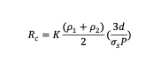
(5)
Where σs is the yield stress, P the contact pressure, and d the surface film thickness. Increasing the electrode force reduces Rc, thereby decreasing local heat generation but improving temperature uniformity across the interface.
Mechanical Interaction:
The mechanical collapse of the projections is essential for achieving proper metallurgical bonding. The synchronization between the softening of the material and the application of the compressive force determines the final weld quality. If heating occurs too rapidly, molten material may be expelled from the joint area, whereas insufficient pressure leads to poor contact and incomplete bonding.
Automation and quality control
Automation enhances process repeatability and throughput. Patnaik’s automated CDW system used a microprocessor-based controller to coordinate charging, part loading, electrode movement, and discharge. The system achieved cycle times below one second per weld, suitable for high-volume assembly of electrical components.
Modern CDW machines integrate machine vision and data logging, enabling closed-loop control. Voltage–current signatures are compared against reference patterns to detect defects such as incomplete discharge or contact misalignment.
Waveform analysis allows estimation of actual energy delivered, interface resistance evolution, and projection collapse rate, providing a non-destructive quality metric (figure 4).
Industrial applications
Capacitor Discharge Welding finds broad application across modern manufacturing, particularly in sectors where high electrical conductivity, precision, and minimal thermal impact are required. In the electrical and electronics industry, it is extensively used for joining conductive materials such as copper, brass, aluminum, and silver in devices like circuit breakers and relays, where silver contacts are welded to brass or copper carriers to ensure low contact resistance and high current-carrying capacity.
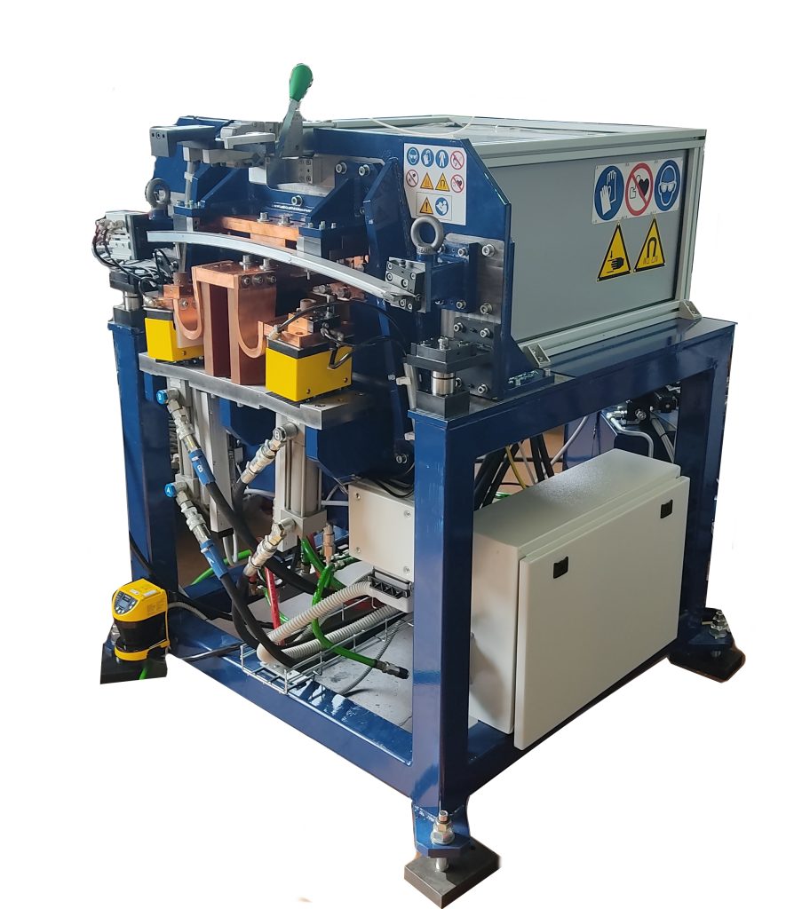
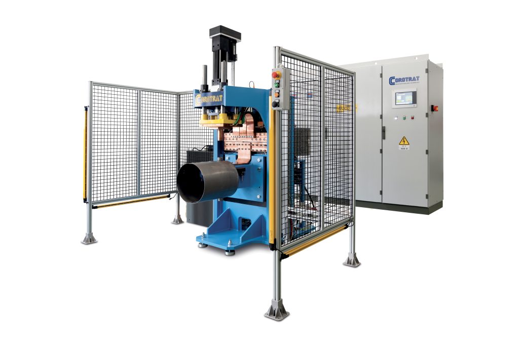
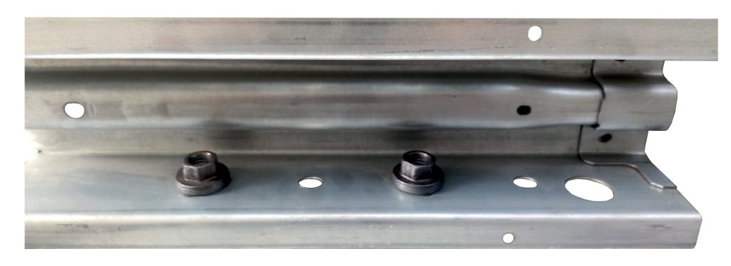
Fig. 5 – CD Welding machine mod. SG40 kJ: CD welder special for welding stainless steel studs on aluminum window guide rail (credit: Corotrat srl)
It is equally valuable for the fabrication of busbars and terminals in power distribution systems and electric vehicles, where its solid-state nature prevents intermetallic growth typical of fusion processes, maintaining long-term electrical reliability. The same principle is exploited in the production of sensor housings and connectors, where thin-walled components require hermetic sealing without the overheating or distortion that accompanies longer welding cycles. In the energy-storage field, CDW provides reliable, repeatable joints between battery cell tabs, typically made of aluminum, copper, or nickel and busbars; its millisecond-scale pulse duration prevents damage to electrode foils and minimizes heat conduction into active materials, which is essential for lithium-ion battery safety and performance.
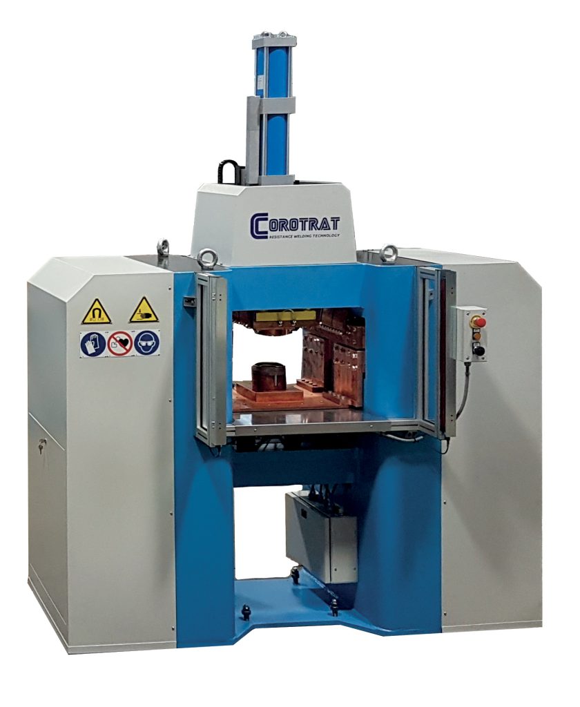
Fig. 6 – CD Welding machine mod. A80 kJ by Corotrat srl; CD welder for automatic clutch gearbox
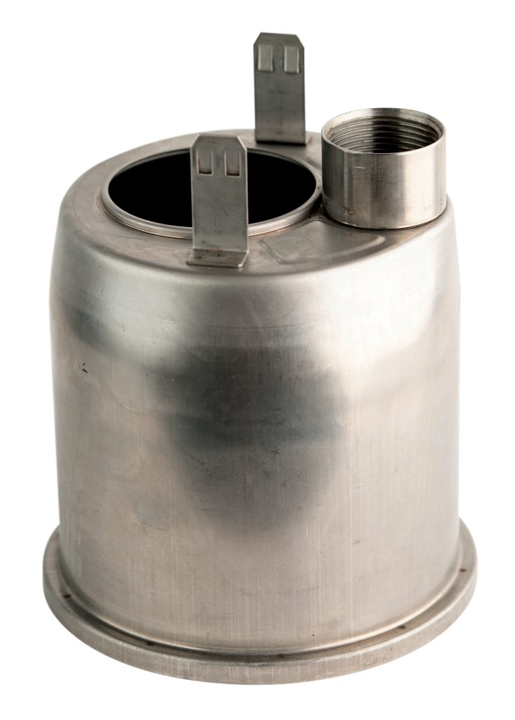
The process has also proven effective for advanced materials, notably in projection-CDW applications used to join oxide dispersion strengthened (ODS) and nano-ferritic alloys such as 14YWT for nuclear reactor cladding, where the rapid solid-state bonding preserves nanoscale oxide dispersions critical to high-temperature strength and radiation resistance. Beyond these specialized uses, CDW is widely adopted in general fabrication tasks including stud welding, sensor mounting, automotive exhaust component assembly, and the manufacture of electrical enclosures. Its short, repeatable energy input, independent of grid voltage fluctuations, makes it highly suited to automated production lines requiring consistent, clean, and distortion-free joints (figures 7 and 8).
Capacitor discharge welding (CDW) offers several notable advantages and engineering considerations, making it a highly efficient and versatile joining method. Its extremely short thermal cycle minimises distortion and residual stresses in the welded components, and the process delivers consistent energy independently of contact resistance. CDW can effectively join dissimilar or plated metals, offering flexibility in material selection, and it achieves an electrical-to-thermal efficiency ratio of around 85–90%. The required equipment is compact and has a low mains power demand. The process lends itself well to automation and requires minimal maintenance. From an engineering standpoint, joint quality depends strongly on surface preparation; the mating surfaces must be clean and flat to ensure uniform resistance. The electrodes, typically made of CuCr or CuW, must be able to withstand erosion at high current densities, and precise alignment is essential, as even slight misalignment can result in asymmetric heating. Additionally, the capacitance and charging voltage must be carefully matched to the electrical and thermal properties of the parts being welded. Process optimisation is often guided by empirical weldability curves, which show the combinations of energy input and applied force that can be used to create strong joints.
Emerging trends and future developments
Advances in supercapacitor technology and solid-state switching are enabling compact, high-frequency CDW systems capable of both pulsed and continuous operation. Research into charge-transfer converter architectures demonstrates the potential for modular welding inverters with efficiencies above 90%.
Digital control systems, AI-based process optimization, and real-time thermal imaging are expected to further enhance consistency. Integration with Industry 4.0 manufacturing environments will allow adaptive energy control based on feedback from weld quality data.
Future developments may also explore hybrid CDW processes, combining capacitive discharge with induction preheating or ultrasonic agitation to extend weldability to composites or multilayer materials.
Conclusions
Capacitor Discharge Welding is a robust, energy-efficient joining process combining the advantages of resistance and solid-state welding. By storing electrical energy and releasing it in milliseconds, CDW generates controlled, localized heating that enables metallurgical bonding with minimal distortion.
Its engineering simplicity, few moving parts, no filler metal, and predictable energy transfer, makes it ideal for automated production. The technology supports a wide range of materials and geometries, including thin foils, plated sheets, and dissimilar metal joints critical in power electronics and energy systems.
Continued improvements in power electronics, capacitor materials, and digital control will further expand its industrial role, making CDW an essential process for the next generation of high-efficiency, electrically integrated manufacturing systems.
(by Andrea Mura, Department of Mechanical and Aerospace Engineering – Politecnico di Torino)


 is an advanced joining technique)