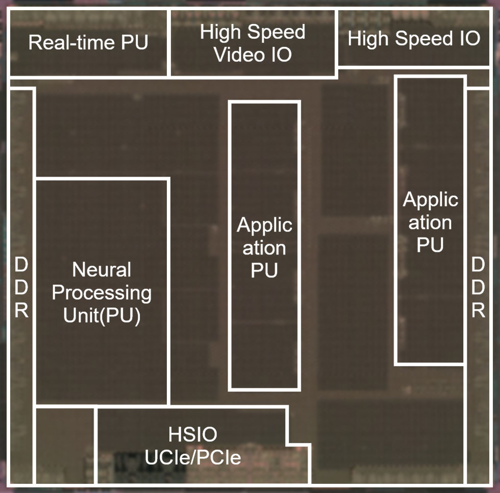
At the International Solid-State Circuits Conference (ISSCC 2026) in San Francisco, Renesas Electronics unveiled a set of System-on-Chip (SoC) technologies designed to meet the performance, safety, and scalability demands of multi-domain automotive control units — a cornerstone of the software-defined vehicle (SDV) era.
The new solutions target central and zonal computing architectures increasingly adopted by carmakers to consolidate electronic control functions and manage AI-intensive workloads.
Automotive SoCs are evolving to support simultaneous execution of numerous domain-specific applications — from ADAS to infotainment — under strict functional safety and power constraints. Renesas’ platform introduces a chiplet-based approach that aims to combine flexibility with safety compliance at ASIL D level.
The proprietary architecture integrates the open die-to-die UCIe interface with a “RegionID” mechanism to prevent hardware resource interference across chiplets. According to Renesas, this solution enables functional separation and deterministic behavior even under concurrent application loads. Bench testing showed bandwidth levels reaching 51.2 GB/s, approaching intra-SoC transfer rates typical of monolithic designs.
AI processing built for automotive reliability
As artificial intelligence becomes central to automated driving and predictive control systems, SoCs must incorporate larger neural processing units (NPUs) without undermining automotive-grade quality targets. Renesas’ 3 nm SoC prototype introduces a reconfigured clock system that distributes mini clock pulse generators (mCPGs) across sub-modules to reduce latency and maintain synchronization. To counter increased test complexity, the company implemented unified signal paths for both user and test clocks, improving phase alignment and supporting zero-defect production standards.
This architectural refinement allows for higher NPU performance — an essential requirement as AI inference and perception functions migrate from edge ECUs to centralized computing nodes.
Power efficiency and functional safety integration
Power management remains one of the most critical challenges for high-performance automotive processors. Renesas’ design features over 90 power domains, controlled dynamically through split power switch (PSW) architectures. Two types of PSWs — ring and row — cooperate to limit inrush current and balance impedance, reportedly reducing IR drop by about 13% compared with conventional layouts.
Functional safety for the power subsystem is reinforced through independent power control of dual lockstep cores, enabling fault detection even if one processing path fails. Additional features such as loopback signal monitoring and high-stability voltage sensing (via the DVMON module) contribute to long-term reliability and improved tolerance to aging-related drift.
Path toward software-defined vehicles
The technologies described by Renesas are being integrated into the company’s new R-Car X5H SoC, announced earlier this year and built on a 3 nm process. This component is positioned to serve as the computational core for multi-domain ECUs combining automated driving logic, digital cockpit interfaces, and connectivity functions on a single scalable platform.
While commercial deployment timelines have not yet been disclosed, Renesas’ work at ISSCC 2026 underscores the direction of automotive compute evolution — from monolithic ECUs to safety-compliant chiplet architectures optimized for AI, performance scalability, and real-time coordination across domains. For carmakers developing SDVs, such innovations could mark a decisive step toward integrating autonomy and digitalization without compromising efficiency or safety.


